









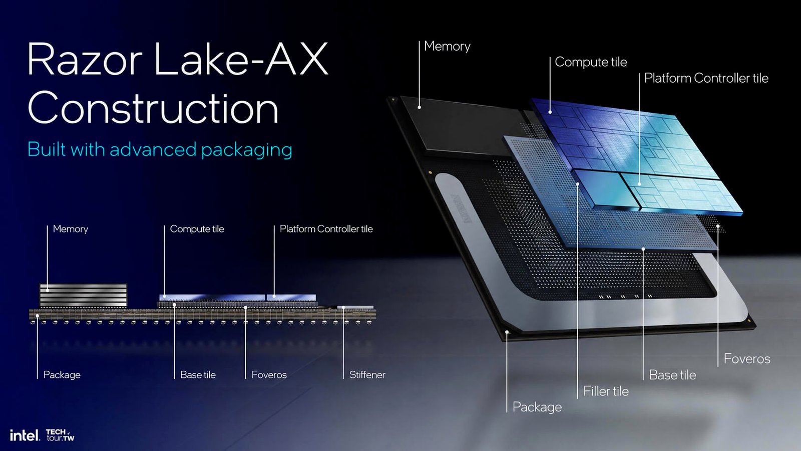
Unveiling the Razor Lake-AX Architecture
Intel recently provided a transformative look into the future of high-performance computing at the Semiconductors Powering Humanoids summit in South Korea. Senior Vice President Cho Min-sung introduced the upcoming “Razor Lake-AX” platform, a silicon design engineered to serve as a cornerstone for advanced robotic and mobile AI applications. While the current industry standard revolves around the transition to Intel’s Panther Lake series, the Razor Lake-AX architecture represents a departure from standard mobile constraints, prioritizing extreme throughput and localized AI processing capabilities.
The primary architectural achievement of Razor Lake-AX is its massive AI compute capability, delivering 700 TOPS (Tera Operations Per Second) on the silicon die. When measured at INT8 or FP8 precision, this platform offers a performance increase of 3.88 times compared to the Panther Lake mobile chips, which currently top out at 180 TOPS. This leap in performance is not merely an iterative gain; it signifies a fundamental shift in how Intel approaches System-on-Chip (SoC) design, integrating substantial CPU complexes with massive, high-performance integrated graphics units.
Harnessing Xe3 Graphics for Extreme Throughput
At the heart of the Razor Lake-AX platform lies the next-generation Xe3 graphics architecture. Intel’s strategy involves two distinct configurations for the integrated GPU: a standard 16-core version and a flagship SKU that scales up to 32 Xe3 GPU cores. This configuration is a significant escalation in graphical and parallel processing density. To put this into perspective, the flagship 32-core iteration is projected to deliver performance nearly three times greater than the current Arc B390, which currently serves as the graphical backbone of the Panther Lake (PTL) lineup.
The physical footprint of this graphical engine is substantial, with the GPU die measuring approximately 162.84 mm². Such dimensions highlight the need for advanced packaging technology. Given the size and complexity of the GPU die alongside the CPU cluster, Intel will likely rely on its proprietary EMIB (Embedded Multi-Die Interconnect Bridge) and Foveros 3D packaging technologies. These methods allow Intel to interconnect various chiplets, ensuring high-speed communication between the compute blocks while maintaining thermal stability and signal integrity.
The Return of On-Package Memory
A noteworthy development in the Razor Lake-AX roadmap is the reintroduction of on-package memory. Previously, Intel suggested that the Core Ultra 200V “Lunar Lake” architecture would be the final design to utilize soldered, on-package memory. However, the performance requirements of the 700 TOPS AI compute target necessitate extreme memory bandwidth and low latency that standard board-level DIMMs struggle to provide. Consequently, Intel has opted to integrate LPDDR5X or LPDDR6 memory directly onto the package for the AX series.
This decision reflects a growing trend in high-performance computing where proximity between data storage and processing units is paramount. By eliminating the distance between the memory controllers and the DRAM, Intel reduces latency and power consumption. This configuration is particularly beneficial for the rapid inferencing required by humanoid robotics and real-time AI processing, where every nanosecond of memory access overhead directly impacts system responsiveness.
Advanced Packaging and Socket Density
Beyond the internal logic, the physical specifications of the Razor Lake-AX highlight its position as an enterprise-grade mobile powerhouse. The platform is slated to utilize a BGA-4326 package featuring 4,326 pins. This pin count is comparable to Intel’s current Xeon server-class processors, signaling that Razor Lake-AX is designed to handle high current, complex power delivery, and massive data I/O requirements that exceed typical consumer hardware constraints.
The high pin count is a necessity for a chip of this magnitude. As Intel moves toward denser, more capable SoCs, the infrastructure required to power and communicate with these chips must scale accordingly. This BGA-4326 socket layout serves as a technical indicator of the chip’s power-hungry, high-performance nature, suggesting that while it may appear in mobile form factors, its operational profile will resemble high-end workstation or server hardware.
Long-term Strategic Roadmap
Intel’s decision to pursue the Razor Lake-AX line follows a reorganization of its internal development priorities. While there was earlier speculation surrounding a “Nova Lake-AX” platform—which aimed to feature 48 Xe3 cores alongside a 28-core CPU cluster—that project has been paused. Instead, Intel has positioned the AX-series initiative to follow the commercial debut of the Nova Lake generation.
This strategic shift ensures that Intel can refine its 3D packaging and Xe3 manufacturing processes before the Razor Lake-AX arrives in 2028. By pushing the launch window to 2028, Intel allows for the maturation of the AI software ecosystem, ensuring that developers have the tools required to fully leverage the 700 TOPS on-die capability. As the industry looks toward the next wave of autonomous hardware, Intel’s Razor Lake-AX positions itself as the primary engine for the compute-heavy future of robotics and edge-AI integration. The platform serves as a vital bridge between modern silicon limitations and the requirements of future, intelligence-driven compute tasks.
Disclaimer: This content is auto-generated for informational purposes only.
Source: Read Original News