









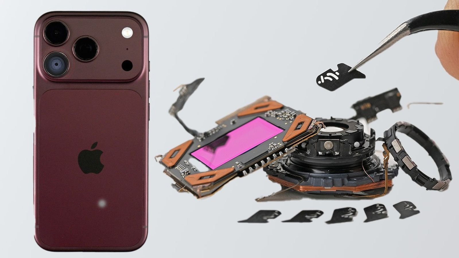
Unveiling the Internal Architecture of the iPhone 18 Pro
The recent release of the iPhone 18 Pro and Pro Max has prompted an immediate deep dive into their internal hardware configurations. iFixit has conducted a comprehensive teardown of these devices, revealing a mixture of incremental refinements and significant structural changes. By stripping away the outer glass and metallic housing, the process highlights how Apple is balancing the demands of high-performance internal components with the logistical constraints of a compact smartphone form factor.
For the eSIM-only models sold in major markets such as the United States, Japan, and several countries in the Middle East, the teardown confirms specific battery energy densities. The iPhone 18 Pro registers at 4,288 mAh, representing a modest 0.8 percent increase over the 4,252 mAh capacity found in its predecessor. However, the iPhone 18 Pro Max showcases a more substantial upgrade, reaching 5,567 mAh, a 9.4 percent increase over the 5,088 mAh found in the iPhone 17 Pro Max. These figures clarify the hardware reality for those purchasing the latest iteration, confirming that the larger model benefits significantly more from recent space-optimization efforts.
Advanced Thermal Management and Component Placement
One of the most noteworthy findings in the teardown is the implementation of a larger vapor chamber. As mobile processors increase in frequency and capability, thermal throttling becomes a primary bottleneck for sustained performance. The inclusion of an expanded cooling surface indicates that Apple is prioritizing long-term stability during intensive tasks like high-resolution gaming, 8K video processing, or augmented reality rendering. By better dissipating heat away from the logic board, the internal system can maintain peak performance metrics for longer durations without requiring a reduction in clock speed.
However, this thermal efficiency comes with a trade-off regarding internal geometry. The NAND flash memory storage has been relocated to reside within the dual-layer logic board. From a manufacturing perspective, this creates a more cohesive, space-saving unit. Conversely, for the repair industry, this design shift introduces complications. Integrating storage directly into the logic board architecture limits the accessibility of this component, making data recovery or specialized storage upgrades significantly more challenging for independent technicians.
Mechanical Hurdles and Structural Integrity
The iFixit analysis uncovered a concerning trend regarding the screen assembly. During the disassembly process, the plastic frame surrounding the display exhibited a susceptibility to cracking and detachment on three out of four units tested. This behavior stands in contrast to previous generations, which typically demonstrated more predictable failure modes during service. While the organization acknowledged that a larger sample size is required to determine if this is a systemic manufacturing defect or a result of specific material fatigue during the opening process, it presents a potential hurdle for repairability.
This structural vulnerability emphasizes the risks associated with the increasingly complex adhesives and sealing materials used to maintain IP-rated water and dust resistance. As manufacturers utilize stronger, more permanent bonding agents to seal devices, the mechanical force required to open them can occasionally result in collateral damage to the frame or display bezels. The iPhone 18 Pro models appear to be particularly sensitive to these pressures at the current stage of production.
Impact on Future Repairability
The combination of the NAND relocation and the fragility of the screen frame underscores a broader trajectory in smartphone engineering. Design teams are increasingly prioritizing the integration of components into a single, high-density stack to maximize battery volume and thermal efficiency. While these efforts yield superior user-facing performance and longevity, they effectively shift the focus away from field repairability.
The use of the dual-layer logic board, while essential for fitting the advanced camera sensors and the upgraded vapor chamber, effectively turns the motherboard into a monolithic component. When storage components are soldered into this complex board, the traditional practice of independent part replacement becomes functionally obsolete. This presents a shift in the ownership experience, where the hardware is designed for its initial lifespan rather than long-term modular maintenance.
Camera System and Variable Aperture Technology
Beyond the logic board and battery, the teardown highlights the implementation of the new variable aperture system. This technical addition allows the camera to adjust the physical opening of the lens, providing users with greater control over depth of field and light intake in varied environments. By integrating a physical iris-like mechanism into the camera module, Apple has managed to maintain the exterior profile of the device while offering features previously reserved for dedicated mirrorless cameras.
This system relies on a set of miniaturized actuators that adjust the aperture blades with high precision. The presence of these motors and mechanical parts within the already crowded camera array explains the necessity for the internal layout changes observed by the teardown team. As mobile photography continues to converge with professional camera capabilities, the structural complexity of these modules will likely remain a focal point of future teardowns. The iPhone 18 Pro demonstrates that while the physical exterior remains deceptively similar to previous versions, the internal mechanical demands are evolving at a rapid pace to accommodate the high-fidelity optics that users now expect from their mobile devices.
Disclaimer: This content is auto-generated for informational purposes only.
Source: Read Original News