









The Evolution of Hardware Security in Microcontrollers
The RP2350 microcontroller, widely recognized for its robust performance and flexible architecture, was engineered with significant security considerations. The Raspberry Pi Foundation integrated several defense mechanisms into the silicon, including secure boot sequences, the ARMv8-M TrustZone architecture, and hardware-based glitch detection. These features were designed to isolate secure execution environments from non-secure ones and to prevent traditional physical attacks, such as voltage fault injection, where an attacker manipulates power input to force a processor to skip instructions or bypass security checks.
Despite these layered defenses, the security community continues to test the limits of these chips. The Ledger Donjon security research team recently conducted an in-depth analysis of the RP2350, moving beyond software-based vulnerabilities to explore the physical limitations of the chip’s security boundary. This investigation highlights the persistent reality that hardware, when subjected to extreme diagnostic measures, remains susceptible to sophisticated physical manipulation.
Decapsulation and Die-Level Analysis
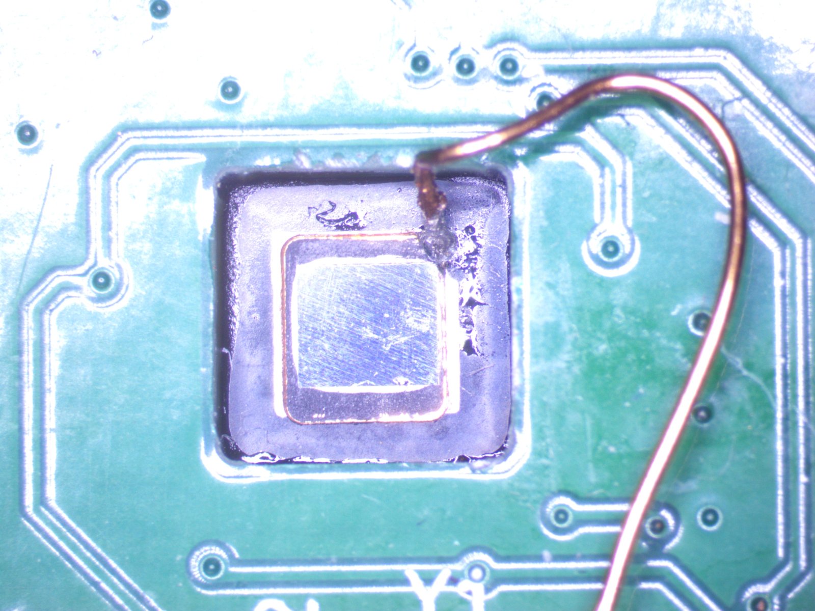
To understand the internal logic of the RP2350, the Ledger Donjon team performed a process known as decapsulation. This involves removing the protective plastic resin (epoxy package) that encapsulates the silicon die. Once the die was exposed, the researchers utilized photon-emission electron microscopy to map the internal layout of the chip. This highly technical procedure allows researchers to identify the physical location of specific registers and logic gates responsible for security features.
The process of locating the debug enable register was essential to the subsequent attack. By correlating the physical layout of the die with the logical operation of the chip, the researchers could pinpoint the exact coordinates where a physical fault could be introduced. This step requires immense precision and expensive laboratory equipment, as the features on modern silicon dies exist at the nanometer scale.
The Mechanism of Laser Fault Injection
Laser Fault Injection (LFI) is a specialized technique that involves focusing a high-energy laser beam onto a precise location of an integrated circuit. Unlike voltage glitching, which affects the entire chip, LFI is surgical. In the case of the RP2350, the researchers prepared a chip by grinding down the backside of the silicon wafer. By shining an infrared laser through the substrate from the rear, they could influence the logic states of transistors without needing to penetrate the complex metal layers on the front of the die.
The laser acts by generating localized electron-hole pairs within the silicon, effectively causing a transient fault that can flip the state of a single bit. By targeting the register that governs the debug interface, the researchers were able to force the chip into an unauthorized state. Despite the chip’s built-in glitch detection, which monitors for sudden fluctuations in electrical parameters, the laser attack successfully bypassed these controls because it acted on a micro-scale level that the chip’s monitoring hardware was not equipped to detect or mitigate.
Bypassing Security to Access Secret Data
The objective of this research was to validate the effectiveness of the chip’s security perimeter by attempting to access a 128-bit secret key. This key was placed in memory as part of a formal security challenge issued by the Raspberry Pi Foundation. Once the researchers successfully manipulated the debug register via LFI, they gained read access to the chip’s secure execution zone.
After successfully injecting the fault, the team performed a device reset while maintaining the debug connection. With the security gate effectively held in an open state by the persistent result of the laser fault, they extracted the 128-bit secret from memory. This process confirms that the debug protection mechanism, while sound in its logic, is physically vulnerable when an attacker possesses the tools to manipulate silicon states directly.
The Persistent Arms Race in Hardware Security
This research serves as a reminder of the ongoing cycle between those who secure hardware and those who challenge it. The Raspberry Pi Foundation’s inclusion of glitch detection is a significant step forward for affordable microcontrollers, as it raises the cost of entry for would-be attackers. However, the Ledger Donjon project required approximately 250,000 USD in specialized equipment, including high-precision lasers and advanced microscopy tools.
For the average user or developer, the RP2350 remains a highly secure platform for most standard applications. The necessity of a quarter-million-dollar laboratory setup and the destruction of a test chip to perform the attack indicates that the barrier to entry remains high. This study does not undermine the functionality of the RP2350, but rather clarifies the boundary between consumer-grade security and state-level forensic analysis.
Future Implications for Embedded Systems
As hardware security continues to mature, manufacturers must account for the reality that physical access is the ultimate vulnerability. The ability to perform LFI on such a widely available chip reinforces the importance of using hardware-backed security not just as a static wall, but as one part of a defense-in-depth strategy. This includes obfuscating memory, using encrypted firmware, and implementing hardware-software co-design that minimizes the impact of potential local faults.
The findings from this analysis provide valuable data for engineers designing secure Internet of Things (IoT) devices. By understanding how sophisticated entities attack modern silicon, designers can better appreciate the trade-offs between cost, accessibility, and physical robustness. While no chip can be considered truly unhackable, the research performed by the Ledger team underscores the technical requirements necessary to bypass modern security, effectively setting a new benchmark for what constitutes “secure” hardware in the current technological landscape.
Disclaimer: This content is auto-generated for informational purposes only.
Source: Read Original News