









Applied Materials Unveils $5 Billion Strategic Investment to Supercharge India’s Semiconductor Ecosystem
New Delhi – In a move that signals a transformative shift for India’s burgeoning electronics manufacturing sector, Applied Materials has announced a massive $5 billion investment commitment over the next decade. The announcement, made at the prestigious SEMICON India 2026 conference in New Delhi, marks a pivotal milestone in the country’s ambition to emerge as a global hub for semiconductor research, design, and manufacturing.
Building a Global Research Powerhouse
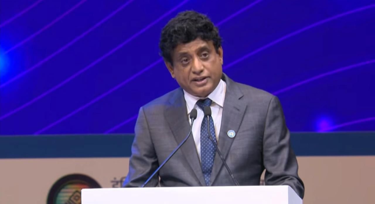
Dr. Prabu Raja, President of the Semiconductor Products Group at Applied Materials, outlined a visionary roadmap during his keynote address, emphasizing the company’s commitment to integrating India more deeply into the intricate global chip supply chain. Central to this strategic investment is the development of a state-of-the-art, 140-acre advanced semiconductor research park.
This facility is expected to serve as a nerve center for next-generation chip innovation. By fostering a collaborative environment for cutting-edge materials engineering and process technology, the research park aims to accelerate the commercialization of new semiconductor solutions while addressing complex challenges in miniaturization and power efficiency.
“This initiative is about more than just capital expenditure; it is about building a sustainable, high-tech ecosystem that empowers local talent and fosters global partnerships,” Dr. Raja stated during the session.
Scaling Workforce and Supply Chain Capabilities
Beyond physical infrastructure, the company has pledged to significantly expand its human capital and operational footprint within the country. The roadmap includes a plan to double its India-based research and development workforce by 2035. This move is designed to harness the nation’s vast pool of engineering talent, particularly in the fields of software, systems architecture, and materials science.
Furthermore, Applied Materials intends to bolster its supply chain capacity by tenfold. By localizing more of its manufacturing and assembly processes, the company aims to reduce reliance on external nodes and stabilize the supply of critical semiconductor equipment. This strategic expansion is anticipated to trigger a ripple effect, encouraging upstream and downstream suppliers to set up operations in India, thereby strengthening the entire value chain.
Strengthening India’s Semiconductor Ambitions
The announcement comes at a time when India is aggressively pursuing its “Semicon India” vision, backed by various government incentives aimed at reducing the country’s import dependency for electronic components. Analysts believe that Applied Materials’ commitment provides a significant vote of confidence in India’s policy framework and long-term economic stability.
By positioning India as a primary node in its global operations, Applied Materials is not only diversifying its geographic footprint but also leveraging the country’s growing expertise in digital transformation. The integration of this research park into the global landscape will likely facilitate a more seamless flow of technology and knowledge transfer between international experts and local specialists.
As the industry moves toward more complex 3nm and 2nm manufacturing processes, the presence of a robust research base in India will be vital. With this $5 billion injection, Applied Materials is setting the stage for India to move from being an assembly-focused market to a premier destination for high-end semiconductor innovation, placing the nation firmly on the map of the global semiconductor narrative.
Disclaimer: This content is auto-generated for informational purposes only.
Source: Read Original News