










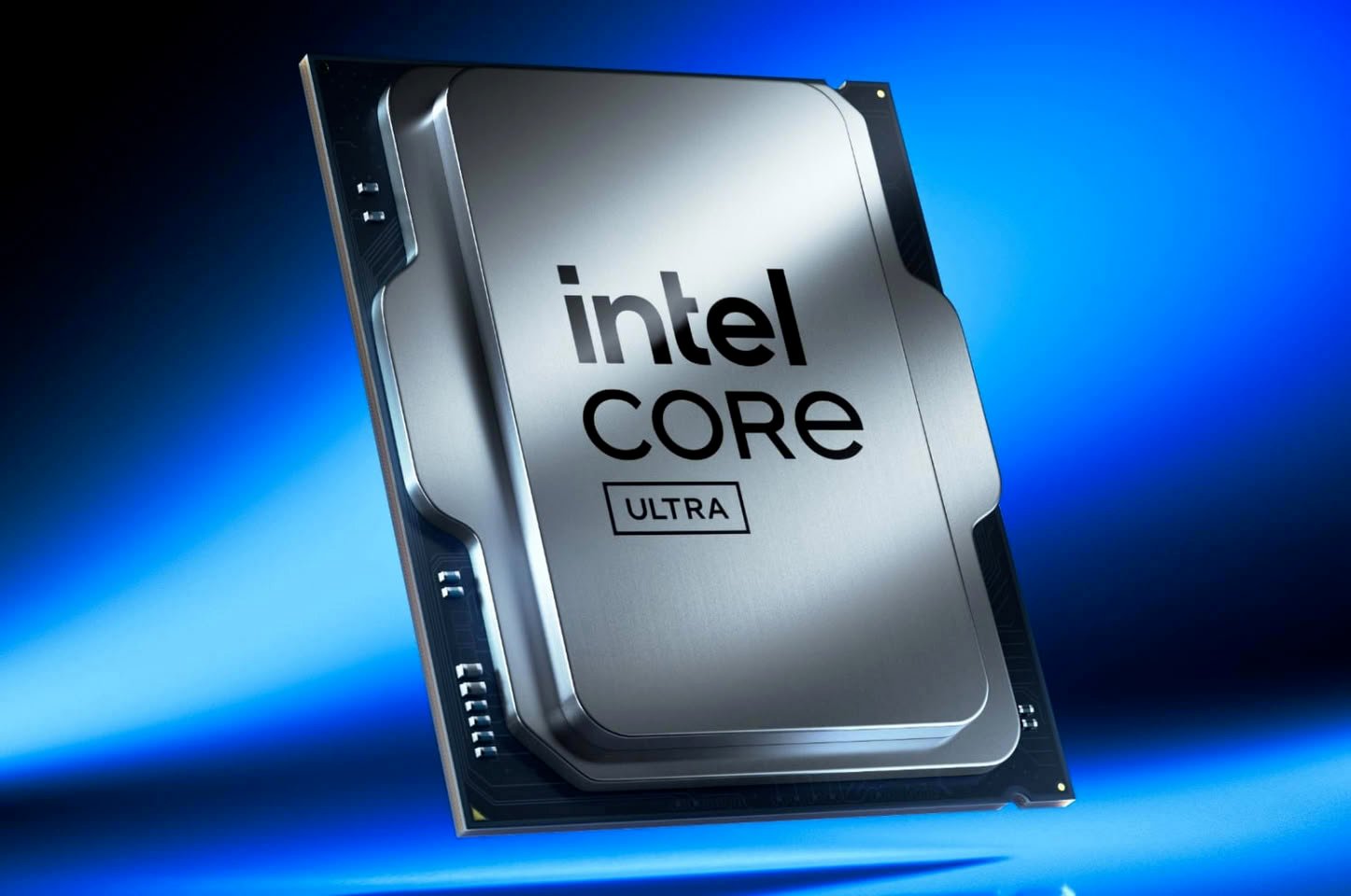
The Emergence of Nova Lake-S Architecture
Intel’s pursuit of microarchitectural efficiency and performance density continues with the emergence of the Nova Lake-S platform. Recent data captured from the OpenBenchmark testing suite has provided a technical window into the development of this next-generation silicon. A processor identified under the “NVL” designation, labeled as “Intel 0000,” confirms that the company is actively testing a 28-core variant. This discovery is significant not only for the raw performance metrics it hints at but also for the structural shift it implies for Intel’s future high-performance desktop (HPT) offerings.
The “Nova Lake-S” identifier points to a single-compute die architecture, which simplifies the manufacturing process and reduces latency between disparate core clusters compared to traditional multi-chiplet configurations. By consolidating these components onto a single die, Intel appears to be prioritizing signal integrity and power efficiency, two critical variables for high-frequency operations.
Decoding the 28-Core Configuration
A core count of 28 represents a sophisticated heterogeneous arrangement. Based on current industry analysis and the provided technical data, this configuration is expected to follow the company’s hybrid architecture philosophy. It likely consists of 8 high-performance P-cores (Performance cores), 16 high-efficiency E-cores (Efficiency cores), and 4 dedicated LPE-cores (Low-Power Efficiency cores).
This tri-tier architecture allows the processor to distribute workloads with extreme precision. The LPE-cores are designed to handle background tasks and low-intensity operations without engaging the high-power P-cores, which serves to preserve energy and thermal headroom. Simultaneously, the 16 E-cores provide massive throughput for multi-threaded applications like video rendering or heavy compilation, while the 8 P-cores handle latency-sensitive instructions such as gaming or single-threaded software execution. This granular approach to resource management is essential as modern software environments become increasingly complex and demanding.
Engineering Milestones and Clock Speeds
The benchmark reports a boost frequency of 5.2 GHz for the Nova Lake-S sample. While this clock speed is competitive, it is imperative to view this figure through the lens of engineering validation. The processor in question is an early-stage engineering sample, meaning it is operating under firmware and power parameters designed primarily for stability and diagnostic testing rather than final retail performance.
Engineering samples often feature internal power limits and clock frequency caps that differ significantly from the final boxed units. It remains unclear whether 5.2 GHz represents the maximum boost capability of a single core or a sustained all-core frequency. Regardless, the ability of this architecture to hit such speeds on an early BIOS build on an NVL-S reference platform indicates that the underlying silicon fabrication is yielding promising results. The use of an Ubuntu 26.04 environment further confirms that this is likely an internal testing process, where engineers are stress-testing the architecture against Linux-based compute workloads, graphics APIs, and OpenCL benchmarks.
Transitioning to New Naming Schemes
The appearance of the “Intel 0000” identifier serves as the first empirical evidence that the company is moving toward a four-digit SKU naming convention. For years, the industry has grown accustomed to the three-digit system, which has become increasingly crowded as core counts and feature sets have expanded. The transition to a four-digit system allows for better differentiation between architectural generations and performance tiers.
This change is not merely cosmetic. It reflects the broader evolution of the processor market, where products are no longer defined simply by a clock speed or a model number, but by their integration of neural processing units, specialized media encoders, and complex memory controllers. A four-digit scheme provides the necessary namespace to accommodate the diverse range of Nova Lake-S variants that will eventually reach the consumer and enterprise markets, ensuring that users can easily distinguish between entry-level silicon and the flagship 28-core performance monsters.
Graphics and Compute Capabilities
Beyond the CPU performance, the benchmark results highlight the “Intel NVL-S” integrated graphics. This identifier confirms that the Nova Lake-S platform is designed to be a complete system-on-chip solution capable of handling intensive compute tasks without the immediate necessity for a discrete graphics card. The inclusion of tests such as Quake II RTX, Unigine, and various Hashcat OpenCL workloads suggests that the graphics architecture within Nova Lake is being pushed to its limits.
These compute-focused tests are designed to evaluate how the integrated GPU handles ray tracing, shader execution, and parallel data processing. By testing these capabilities early in the development cycle, Intel is ensuring that the graphics engine can scale effectively with the high-performance CPU cores. This synergy is crucial for modern productivity workflows, where applications are increasingly reliant on GPU acceleration for tasks such as image filtering, AI-driven background replacement, and real-time data visualization.
The Impact of the Nova Lake Platform
The impact of the Nova Lake-S, particularly with its 28-core density and refined architectural balance, will be felt across the high-end desktop space. By moving away from older, less efficient core management systems, Intel is attempting to reclaim performance leadership in a market that has seen significant pressure from competitor silicon.
If the 5.2 GHz frequency is merely a baseline, and the final retail versions see improved power efficiency and higher sustained clocks, Nova Lake-S could represent a substantial generational leap in terms of both instruction-per-clock performance and total system throughput. The integration of LPE-cores and the optimization of the NVL-S platform demonstrate a clear roadmap toward machines that remain quiet and power-efficient during idle or light use, while maintaining the capacity to scale into a computational powerhouse when the task demands it. As development continues, the industry will be watching these benchmarks closely to see how the final retail versions of these “0000” series processors perform in real-world scenarios.
Disclaimer: This content is auto-generated for informational purposes only.
Source: Read Original News