








The Emergence of AMD Gainsborough
The landscape of handheld gaming hardware is currently defined by the Steam Deck, a device that has maintained a dominant market position for over four years. While enthusiasts have spent the last two years speculating about a successor, Valve has remained disciplined in its messaging: a new version will only enter production when the technology allows for a significant generational leap in performance and energy efficiency. Recent leaks regarding a new AMD silicon codenamed “Gainsborough” have reignited this conversation, suggesting that the necessary architectural advancements might finally be nearing commercial readiness.
The moniker Gainsborough is notable due to its historical connection to previous Valve hardware codenames. The original Steam Deck APU was dubbed “Aerith,” and the updated OLED model was referred to as “Sephiroth.” In the narrative of the video game Final Fantasy VII, Aerith Gainsborough is a central character, leading many observers to conclude that the naming convention is a direct nod to a continued partnership between Valve and AMD. However, technical analysis suggests that while the name is suggestive, the reality behind the silicon is more complex.
Technical Specifications and Process Nodes
According to reports from industry trackers, the Gainsborough chip appears to be a semi-custom unit developed for a specific partner, utilizing TSMC’s N3P manufacturing process. The N3P process is a critical element of this development, as it represents a mature iteration of the 3nm node, offering substantial improvements in transistor density and power leakage reduction compared to older 7nm or 6nm designs. For a handheld device where thermal headroom is the primary constraint, moving to a denser, more efficient node is the most effective way to extract higher frame rates without causing the device to overheat or suffer from rapid battery depletion.
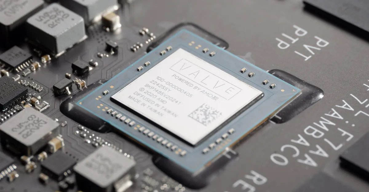
Import and export records indicate that AMD has already begun circulating test hardware for the Gainsborough platform. This stage of validation is typical when manufacturers prepare for a high-volume product launch. These records further reveal that the chip utilizes an FF6 package measuring 25mm by 25mm. This physical footprint aligns with rumored dimensions for AMD’s upcoming Ryzen Z3 and Z3 Extreme processors, which are projected to target a 15-watt thermal design power (TDP). This power envelope is synonymous with the current Steam Deck architecture, suggesting that any device utilizing the Gainsborough chip would be built to operate within similar portable parameters.
Challenges in Identifying the Successor
Despite the excitement surrounding the Gainsborough codename, skeptics point out several factors that complicate the assumption that this chip is destined for a Steam Deck 2. First, the historical record of semi-custom silicon reveals that chips designed for one purpose often find their way into entirely different products. The original Steam Deck’s “Aerith” APU, for example, was rumored to be the intended engine for a high-end augmented reality headset before that project was pivoted or canceled. Valve subsequently adapted the existing design to fit the handheld form factor. Consequently, the mere existence of a semi-custom chip does not guarantee its intended home.
Furthermore, industry insiders have clarified that the Final Fantasy naming convention for these chips was actually an internal AMD decision rather than a directive from Valve. While the link to previous chips is charming, it may be more indicative of an AMD product family naming internal logic rather than a specific confirmation of a partnership with Valve. When compared to the physical dimensions of the original Aerith silicon, the 25mm by 25mm footprint of the Gainsborough chip is notably larger. If the next iteration of the Steam Deck requires extreme miniaturization to accommodate a larger battery or improved cooling, this larger chip footprint could present a physical hurdle for hardware engineers.
Efficiency and the Generational Leap
The core requirement for a next-generation handheld is efficiency. Gaming at higher resolutions—such as 1080p or 1200p—demands significantly more graphical power than the Steam Deck’s current 800p output. If Gainsborough is indeed intended for a future high-performance handheld, its success will depend on its ability to handle modern ray-tracing APIs and upscaling technologies without exceeding the power limits that define the handheld experience. The shift to the TSMC N3P process is a strong indicator that efficiency is the primary goal, even if the chip size appears slightly larger than previous generations.
A potential shift toward an architecture shared with the Ryzen Z3 series would also offer significant software benefits. Because the Steam Deck relies heavily on a specialized iteration of Linux, maintaining compatibility with standard AMD hardware architectures allows Valve to streamline driver development and kernel optimization. If the Gainsborough chip shares lineage with the Z3 line, it could simplify the process of bringing the latest features of the RDNA graphics architecture to the SteamOS environment, ensuring that the software stack remains performant and stable.
The Future of Handheld Computing
Whether the Gainsborough chip is destined for a Valve product or another manufacturer’s handheld, its appearance highlights the rapid evolution of mobile gaming hardware. We are entering a phase where the boundary between mobile-class efficiency and desktop-class graphics capability is thinning. The transition to advanced nodes like N3P will likely dictate the next two years of handheld innovation, allowing devices to push higher graphical fidelity while maintaining the three-to-four-hour battery life that users have come to expect.
While Valve has not issued a formal confirmation regarding the development of a successor to the Steam Deck, the discovery of Gainsborough provides a tangible point of interest. It represents the type of technological maturation that Valve has publicly demanded before committing to a new generation of hardware. As validation testing continues, the industry will monitor the performance metrics of these chips closely to determine if the “generational leap” in performance is truly ready to move from the factory floor to the end user. Regardless of the specific device it eventually powers, Gainsborough is a reminder that the handheld market is not slowing down, and the next leap in performance is likely closer than many anticipated.
Disclaimer: This content is auto-generated for informational purposes only.
Source: Read Original News