










SK Hynix Unveils Next-Gen HBM Strategy: Tackling the Thermal and Architectural Limits of 3D Stacking
At the Hot Chips 2026 conference, SK Hynix provided a deep dive into the future of memory architecture, detailing how it plans to navigate the mounting technical hurdles of high-bandwidth memory (HBM). As the demand for AI and high-performance computing (HPC) continues to skyrocket, the company is doubling down on advanced packaging technologies to push the boundaries of capacity, bandwidth, and power efficiency.
The Challenge of Scaling HBM
Current HBM solutions rely on a 3D-stacked structure, connecting multiple core DRAM dies to a base die via Through-Silicon Vias (TSVs). Today’s state-of-the-art reaches a 16-high (16-Hi) stack configuration. While effective, the path toward even higher stacks and denser performance faces a “thermal wall.”
According to SK Hynix, every two generations of HBM performance improvement result in a 2.2x increase in thermal burden. To sustain this, the company is moving beyond conventional assembly methods, shifting focus toward hybrid bonding and specialized cooling innovations.
Bridging the Gap: MR-MUF and Hybrid Bonding
SK Hynix currently employs two primary packaging methodologies:
- TC+NCF (Thermo-Compression + Non-Conductive Film): Favored for its superior resistance to die warpage, though it suffers from lower productivity and higher thermal resistivity.
- MR-MUF (Mass Reflow + Molded Underfill): Known for high productivity and better thermal performance, but requires precise control to manage potential chip warpage.
For its latest 16-Hi HBM3E solutions, the company has introduced an “Advanced MR-MUF” process that features enhanced warpage control and finer pitch integration. However, the long-term roadmap points toward Hybrid Bonding. This next-generation technique allows for a significantly smaller TSV pitch (below 18 microns) and provides a 35% reduction in thermal resistance, proving essential for stacks that aim to exceed 16 layers.
Innovation in Cooling and Logic
To combat localized heating—a common failure point in modern GPU-coupled memory—SK Hynix is developing its proprietary I-HBM (Integrated HBM) technology. By embedding high-thermal-conductivity components directly into the HBM D2D PHY area, the company can create dedicated heat paths that reduce thermal resistance by over 30%.
Furthermore, SK Hynix is exploring deeper integration with logic foundries. By optimizing power delivery networks (PDN) and implementing “power TSVs” throughout the memory stack, the company aims to mitigate the voltage drop and power delivery challenges inherent in such dense, high-speed architectures.
The Future of 3D Integration
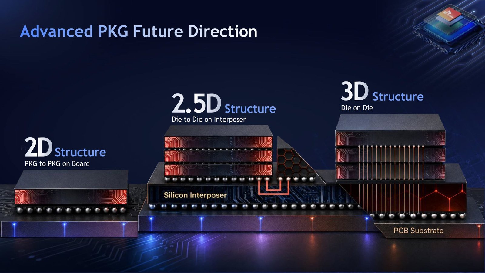
The company’s roadmap also highlights a shift toward true 3D integration, where HBM will eventually be stacked directly on top of accelerators. This transition is being supported by collaboration with industry leaders and the adoption of cutting-edge packaging substrates like Intel’s EMIB (Embedded Multi-die Interconnect Bridge) and variants of TSMC’s CoWoS (Chip-on-Wafer-on-Substrate) technologies.
As SK Hynix sets its sights on 16-to-20-high stacks, the success of these memory modules will depend on the tight co-optimization of materials, logic processes, and customer-specific interposer designs. With the industry’s hunger for bandwidth showing no signs of slowing, SK Hynix’s pivot toward more robust, thermally efficient packaging represents a critical evolution for the next generation of AI hardware.